Home
Resources
Resources

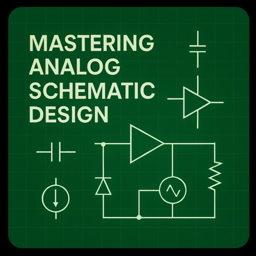
Mastering Analog Schematic Design
Explore best practices for precise analog schematic designs in nanoelectronics.
Analog schematic design is crucial in developing robust integrated circuits. It involves creating detailed circuit diagrams that represent electronic components and connections, ensuring optimal performance and signal integrity. Designers use specialized software like Cadence Virtuoso to capture hierarchical schematics, manage design rule compliance, and prepare for simulations. Accurate analog schematics facilitate efficient verification and successful tape-out processes, minimizing errors and silicon re-spins. Emphasis is placed on low power consumption, noise reduction, and component matching techniques to achieve high-quality analog circuits within space constraints.
Effective Digital RTL Design Guide
Learn flexible RTL design methods for efficient digital circuit implementation.
Register Transfer Level (RTL) design describes digital circuit functionality using hardware description languages such as Verilog or VHDL. Effective RTL design focuses on modularity, timing optimization, and minimizing logic complexity. Designers create synthesizable code representing registers, logic gates, and data paths compatible with target fabrication technologies. Creating reusable RTL modules streamlines SoC development. Simulation environments verify RTL functionality and performance before progressing to physical layout, ensuring first-time-right silicon success. Adhering to coding guidelines and testbench integration enhances design robustness for consumer, telecom, and automotive applications.

Custom Layout Design and Verification
Discover techniques for creating silicon-efficient full-custom IC layouts.
Custom layout design translates circuit schematics into precise transistor-level physical representations. Using tools like Cadence Virtuoso and Mentor Calibre, designers ensure layouts comply with foundry-specific Design Rule Checks (DRC) and Layout Versus Schematic (LVS) verification. Techniques such as common-centroid and matched device layouts reduce variability and improve analog performance. Customized routing, parasitic extraction, and EM/IR safety are critical for high-yield manufacturing. Post-layout simulations validate functionality and performance under cornermost operating conditions, enabling quick tape-out and production success across technology nodes from 180nm to 5nm.
FPGA Emulation in Nanoelectronics
Understand FPGA emulation for prototyping and validation of integrated circuits.
FPGA emulation provides a practical method for prototyping digital and mixed-signal integrated circuit designs by mapping RTL code onto Field Programmable Gate Arrays. This approach allows pre-silicon validation of functionality, timing, and system interactions in a real hardware environment, significantly reducing development risk and cost. FPGA emulation facilitates early software development, debug of complex SoC behaviors, and helps ensure first-time silicon success. It integrates with simulation and testbench environments to thoroughly verify designs before tape-out, especially in consumer and telecom sectors embracing advanced semiconductor technologies.
Frequently Asked Questions
Request a Quote
Fill our form to get tailored nanoelectronics design solutions that meet your project needs efficiently and affordably.
9AM to 6PM
Analog and Mixed-Signal Design
Custom Layout Design and Physical Verification
Digital Design and FPGA Services
PCB Design Service
© 2025 Sudhal Nanoelectronics Services

